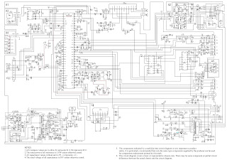
This circuit is a circuit diagram 12V inverter is very easy to build, cheap components that many electronics hobbyists may even already have. Though it is possible to build a more powerful circuit, the complexity caused by the very heavy currents to be handled on the low-voltage side leads to circuits. The circuit diagram of 12v inverter is easy to follow. A classic 555 timer chip, identified as IC1, is configured as an astable multivibrator at a frequency close to 100 Hz, which can be adjusted accurately by means of potentiometer P1. It is used to drive a D type flip-flop produced using a CMOS type 4013 IC. This produces perfect complementary squarewave signals (in antiphase) on its Q and Q outputs suitable for driving the output power transistors. The following is a schematic drawing: As the output current available from the CMOS 4013 is very small, Darlington power transistors are used to arrive at the necessary output current. We have chosen MJ3001s from the now defunct Motorola
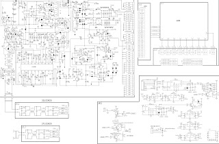
Description Mono high power amplifier is actually a powerful 1400 W, but if this hihgh power amplifier circuit is doubled and you want to create stereo, high power amplifier the necessary components and pcb requires two-fold. So if the stereo high power amplifier 2 X 1400W. Schematic Circuit diagram is still less by looking at the circuit that was so below, the finished circuit has been added with a gains using JRC4558 IC by the two and the picture ic where it can be seen below. For circuit buffers, drivers , and booster use multiple transistors and other components (can be seen listed component ). And high power amplifier project that is so below is just part of the buffer and driver while the booster has not been made. For additional transistors in the booster or high power amplifier end scheme can be found Booster output power amplifier. Circuit Schematic Diagram : Part List : R1_____560Ω R2_____100Ω R3_____2K2Ω R4_____560Ω R5_____1Ω R6_____27KΩ R7_____10KΩ R8_____100Ω R9___


Comments
Post a Comment