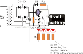
Posts

Showing posts from December, 2016

Fog Lamp Sensor

Image
Fog Lamp Sensor Circuit diagram . For several years now, a rear fog lamp has been mandatory for trailers and caravans in order to improve visibility under foggy conditions. Fog Lamp Sensor Circuit diagram : Fog Lamp Sensor Circuit Diagram When this fog lamp is switched on, the fog lamp of the pulling vehicle must be switched off to avoid irritating reflections. For this purpose, a mechanical switch is now built into the 13-way female connector in order to switch off the fog lamp of the pulling vehicle and switch on the fog lamp of the trailer or caravan. For anyone who uses a 7-way connector, this switching can also be implemented electronically with the aid of the circuit illustrated here. Here a type P521 optocoupler detects whether the fog lamp of the caravan or trailer is connected. If the fog lamp is switched on in the car, a current flows through the caravan fog lamp via diodes D1 and D2. This causes the LED in the optocoupler to light up, with the result that the phototransisto

Ups System mini

Image
This Ups System mini circuit provides an uninterrupted  power supply (UPS) to operate 12V, 9V and 5V DC-powered instruments at up to 1A current. The backup battery takes up the load without spikes or delay when the mains power gets interrupted. It can also be used as a workbench power supply that provides 12V, 9V and 5V operating voltages. The circuit immediately disconnects the load when the battery voltage reduces to 10.5V to  prevent deep discharge of the battery.  LED1  indication  is  provided  to  show  the full charge voltage level of the battery. miniature white LEDs (LED2 and  LED3) are used as emergency lamps during power failure at night.  Mini Ups System Circuit Diagram A standard step-down transformer provides 12V of AC, which is rectified by diodes D1 and D2. Capacitor C1 provides ripple-free DC to  charge the battery and to the remaining circuit. When the mains power is  on, diode D3 gets forward biased to charge the battery. Resistor R1 limits the charging current. Pot

Eighteen Watt Audio Amplifier

Image
18 Watt Audio Amplifier circuit diagram . High Quality very simple unit No need for a preamplifier . Circuit diagram : 18Watt Audio Amplifier Circuit Diagram Amplifier parts: P1____22K  Log. Potentiometer (Dual-gang for stereo) R1___1K  1/4W Resistor R2___4K7 1/4W Resistor R3___100R  1/4W Resistor R4___4K7 1/4W Resistor R5___82K  1/4W Resistor R6___10R  1/2W Resistor R7___R22  4W Resistor (wirewound) R8___1K  1/2W Trimmer Cermet (optional) C1___470nF  63V Polyester Capacitor C2,C5___100µF   3V Tantalum bead Capacitors C3,C4___470µF  25V Electrolytic Capacitors C6___100nF  63V Polyester Capacitor D1___1N4148  75V 150mA Diode IC1___TLE2141C  Low noise, high voltage, high slew-rate Op-amp Q1___BC182  50V 100mA NPN Transistor Q2___BC212  50V 100mA PNP Transistor Q3___TIP42A  60V 6A    PNP Transistor Q4___TIP41A  60V 6A    NPN Transistor J1___RCA  audio input socket Power supply : 18Watt Audio Amplifier Power Supply Power supply parts:   R9___2K2 1/4W Resistor C7,C8___4700µF 25V Electr

Simple Field Strength Meter

Image
This Field Strength Meter is simple and also quite sensitive. It uses an ordinary digital voltmeter to measure RF signal strength up to a few hundred MHz. Simple Field Strength Meter Circuit diagram: Parts List: 1 OA91 Germanium Diode 1 3.3M Resistor 1 100p Capacitor L1 7 turns on a 1/4 inch former (suitable for around 100MHz) Notes: The multimeter should be set to the lowest dc volts range for maximum sensitivity. This is normally 200mV DC for most meters. The circuit works well at VHF (around 100MHz) and was quite pleased with the results. L1 was 7 turns on a quarter inch former with ferrite slug. This covered the UK FM band. A digital multimeter, as opposed to an analogue signal meter offers several advantages in this circuit. First, the impedance of a digital meter is very high, around 10Meg/Volt on most meters. This does not shunt the tank circuit unduly. Second, compared to an analogue meter, very slight differences in signal strength can be more easily observed. Thirdly,a digita

Car Amplifier Care Tips

Image
Car Amplifier Care Tips Amplifier that work as one of the pillars of car audio does have ipandang performance that can not be underestimated. so we need to know a few things to keep our car amplifiers are not easily damaged. The following tips for creating a durable amplifier. 1. To install an amplifier on the audio systems in vehicles to avoid amplifier from moisture, the way while avoiding the base of potential placement into water vapor. so do not get into the inside of the amplifier resulting in damage to the components inside. 2. There is a good amplifier is used or not stored in a long time alias stored in a warehouse because after all the components within it requires a flow of current in accordance with nature as Conductor supply current to the driver other car audio. 3. Inside the vehicle, an amplifier should also be checked periodically, this is to find out the connection cable attached to the amplifier, amplifier kondiso also working actively to your car audio system.

Project of Transformer less Power Supply Circuit Diagram

Image
This circuit will supply up to about 20ma at 12 volts. It uses capacitive reactance instead of resistance; and it doesn't generate very much heat.The circuit draws about 30ma AC. Always use a fuse and/or a fusible resistor to be on the safe side. The values given are only a guide. There should be more than enough power available for timers, light operated switches, temperature controllers etc, provided that you use an optical isolator as your circuit's output device. (E.g. MOC 3010/3020) If a relay is unavoidable, use one with a mains voltage coil and switch the coil using the optical isolator.C1 should be of the 'suppressor type'; made to be connected directly across the incoming Mains Supply. They are generally covered with the logos of several different Safety Standards Authorities. If you need more current, use a larger value capacitor; or put two in parallel; but be careful of what you are doing to the Watts. The low voltage 'AC' is supplied by ZD1 and ZD2

PCB Exposure Switch Timer V2 0

Image
After some modifications on my UV exposure box (scanner) for better UV expose, i decided that a better pcb must me designed for switch timer. The old one had over drilled holes and it was designed and built on my very fist steps. Also the high voltage side from the low voltage wasn’t separated as it needed to be safe. So i redesigned it in a more compact and easier to use pcb. The firmware has been also updated and now you can program the timmer by using the two buttons. The time is calculated by timer interrupt triggering using a 32.768KHz RTC Crystal with better accuracy. The display update also has been changed from static to dynamic. [ ]

1W Audio Amplifier Using NCP2830

Image
This 1w audio amplifier circuit is designed using NCP2830 audio IC manufactured by ON Semiconductor.This audio power amplifier ic designed for portable communication device applications and require few external electronic components. 1W Audio Amplifier Circuit using NCP2830  NCP2830 is capable to provide 1W continuous output power in 8 ohms load.NCP2830 audio power amplifier main features are : high quality audio (THD+N = 0.04%) , low noise: SNR up to 100 dB, overall system efficiency optimization: up to 89% , Superior PSRR (−88 dB): Direct Connection to Battery , Very Low Quiescent Current 7 mA , Optimized PWM Output Stage: Filterless Capability , Selectable gain of 2 V/V or 4 V/V .

Paraphase Tone Controller

Image
As opposed to the widespread Baxandall circuit (dating back to 1952!) a ‘paraphrase’ tone control supplies a straight frequency response as long as the bass and treble controls are in the same position. This unique property makes the ‘paraphase’ configuration of interest if only treble or bass needs to be adjusted - it is not possible to adjust both at the same time! Essentially, it’s the difference in setting of the tone controls that determines the slope of the frequency response, and the degree of bass/treble correction. The circuit is simplicity itself, based on two networks C1-C2-C3/R9-R10-R11 and C5-C6-C7/R12-R13-R14. Picture of the project: Paraphase Tone Controller Circuit The first is for the high frequencies (treble) response, the second, for the low frequencies (bass). The roll-off points have been selected, in combination with C4 and C8, for the sum of the two output signals to re-appear with a ‘straight’ frequency response again at the output. Roughly equal output levels f

SSB Add On For AM Receivers

Image
Given favourable radio wave propagation, the shortwave and radio amateur band are chock-a-block with SSB (single-sideband) transmissions, which no matter what language they’re in, will fail to produce intelligible speech on an AM radio. SSB is transmitted without a carrier wave. To demodulate an SSB signal (i.e. turn it into intelligible speech) it is necessary to use a locally generated carrier at the receiver side. As most inexpensive SW/MW/LW portable radios (and quite a few more expensive general coverage receivers) still use plain old 455 kHz for the intermediate frequency (IF), adding SSB amounts to no more than allowing the radio’s IF to pick up a reasonably strong 455-kHz signal and let the existing AM demodulator do the work. Circuit diagram: The system is called BFO for ‘beat frequency oscillator’. The heart of the circuit is a 455-kHz ceramic resonator or crystal, X1. The resonator is used in a CMOS oscillator circuit supplying an RF output level of 5 Vpp. which is radiated

Bipolar Transistor Tester

Image
This tester is primarily meant to test bipolar transistors. It can indicate the type of the transistor as well as identify its base, collector and emitter pins. The circuit is very simple. The direction of current flow from the terminals of the transistor under test (TUT) is indicated by a pair of LEDs (green-red). An npn transistor produces a red-green-red glow, while a pnp transistor produces a green-red-green glow, depending on the test point that connects to the terminal of the transistor. Emitter and collector are differentiated by pressing pushbutton switch S1 that actually increases the supply voltage of the circuit by about 5.1V. At the heart of the circuit is IC CD4069 (IC3), which oscillates and produces pulses required to test a pair of transistor leads for conduction in both the directions. Different combinations are selected by an arrangement of counter CD4040 (IC1) and bilateral switch CD4016 (IC2). Fig. 1 shows the circuit of the bipolar transistor tester. A pair of LEDs

Frequency doubler with 4069 Circuit

Image
Description  This frequency doubler using a single 4069 hex inverter IC, a frequency doubler can be constructed to give an output pulse train whose frequency is twice that of a squarewave input signal. The signal is applied to the input of N1. It should be a squarewave with a duty-cycle of approximately 50% at level compatible with CMOS logic (3-15V peak to peak depending on supply voltage). The input signal is buffered and inverted by N1, and inverted again by N2, so the outputs A and B of N1 and N2 are squarewave signals 180° out of phase. The output of N1, is differentiated by C1 and R1 and the output of N2 is differentiated by C2 and R2, giving two spike waveforms of C and D, 180° out of phase. The signals are buffered, inverted and shaped by N3 and N4. These are then combined in a NOR gate consisting of D1, D2, R3 and N5, and finally inverted by N6 to give the frequency twice that of the input signal. The circuit will operate over a wide frequency range. With the component values

Simple Subwoofer Lowpass Filter using uA741 Single Op Amp Ic

Image
This is the simplest Sub woofer Low Pass filter Circuit using uA741 single op amp ic . The circuit is very low cost with respect to their work. The cut off frequency of this circuit is 25Hz to 80Hz maximum. Using this circuit , you can easily design a 2.1 Sub-woofer Speaker System at your own Home. The circuit contains very few components.In Pakistan, the cost of this circuit with PCB is Rs:45 The same circuit is working in my own hand made sub-woofer system. So Try this [ ] Parts List:   R1,R3,R4 = 10K 1/4W R2=100K 1/4W CY1,CY2 = 0.22uF Polyester C1,C2 = 10uF/25V Electrolytic IC1 = uA741A Single Op-Amp Ic + 8 Pin Ic Socket 3 Pin Male & Female Connector x 2 2 Pin Male & Female Connector x 1 PCB as in required size 4.5 cm x 3.4 cm

6 12V Variable Regulated Power Supply

Image
This is an adjustable / variable power supply which have adjustable output voltage from 6-12 DC volt. This power supply can be used for general circuit or gadget which require 6 – 12DC voltage to work. Component Parts List: T1 = primary 115[220]/secondary 8 VAC transformer. Center Tap not needed. Q1 = 2N1613, NTE128, or substitute. (TO-39 case) On coolrib! BR1 = 40V, 4A. (Check max current of your mini-drill and add 2A) R1 = 470 ohm, 5% R2 = 1K, 5% P1 = potentiometer, 10K C1 = 1000uF, 25V Notes: C1 filters the noise and spikes off the AC. If you find the circuit output too noisy add another electrolytic capacitor over the output terminals. Value can be between 10 and 100uF/25V. The output voltage is variable with the 10K-potentiometer. The transformer input voltage refer to your home power source. Mount the transistor on heatsink / cooling rib to prevent overheating. Read more http://circuitdiagram.net/6-12v-variable-regulated-power-supply.html

Using a single 7812 IC 12 Volt 30 Amp Circuit Diagram

Image
This is the Using a single 7812 IC - 12 Volt 30 Amp Circuit Diagram simple project. Using a single 7812 IC voltage regulator and multiple outboard pass transistors, this power supply can deliver output load currents of up to 30 amps. Notes: The input transformer is likely to be the most expensive part of the entire project. As an alternative, a couple of 12 Volt car batteries could be used. The input voltage to the regulator must be at least several volts higher than the output voltage (12V) so that the regulator can maintain its output. If a transformer is used, then the rectifier diodes must be capable of passing a very high peak forward current, typically 100amps or more. The 7812 IC will only pass 1 amp or less of the output current, the remainder being supplied by the outboard pass transistors.  As the circuit is designed to handle loads of up to 30 amps, then six TIP2955 are wired in parallel to meet this demand. The dissipation in each power transistor is one sixth of the total

FM Transmitter Circuits The BIG List

Image
Over years we have developed a number of FM transmitter circuits with various aspects. Today I thought of listing all of them here as a single web page, so any one can easily navigate through all the radio transmitter circuits and its schematic diagrams. Simple Two Stage FM Transmitter – This is one of the most simple FM transmitter circuit you can try out on your breadboard. It has two stages served by two transistors Q1 and Q2. The first stage is the preamplifier stage where audio input signal is amplified before modulation. This stage is served by Q1 (BC108). Second stage is the modulation stage in which amplified audio signal is modulated (superimposed to a carrier waver) for transmission. This stage is served by Q2 (2N2369). Carefully observe the schematic diagram before you build this circuit. 200 Meter Transmitter – This one is yet another simple FM transmitter but more stable than the one listed above. The basic functioning of the circuit is same as the above one, two stages

Flip Flop Led Circuit

Image
Flip Flop LED Flip flop circuit is a series of free runing multivibrator given the burden of LEDs on each side of the transition changes its output signal. Flip flop circuit with LEDs is quite simple, that is prepared with 2 units and 2 units of 2N3904 transistor circuit tank circuit composed by the RC circuit.  LED indicators signal a change that is placed on each side of the flip flop will be lit in turn by the fire and extinguished the same as the charge and discharge capacitor. Flip flop circuit is quite simple as shown in the picture below. Flip Flop LED series The working principle is the flip flop over when the series voltage source is given then the 10uF capacitor will be charged through R 470 and the LED will then be forwarded to triger the transistor base so that the transistor will turn ON and LEDs. this occurs alternately on each side, so that the LED light will illuminate in turn as well.

Auto LED Taillight for a Bike

Image
This is a circuit for automatically switching off and LED taillight for a bike. The backlight turns on by movement (in the dark). After about 20 minutes of inactivity, the backlight is switched off again. So you cannot forget to turn off the backlight so that you are less likely surprised by batteries.  Auto LED Taillight Circuit Diagram S1 is a motion switch. When the switch closes C1 is charged. Therefore FET switches T1 and burn the LED. T1 can however only enabled when R3 is sufficiently high resistance, or when it is dark. R1 C1 discharge slowly so that after about 20 minutes the FET turns off and the LED goes out. The circuit may be built into the housing of a rear light on the battery that is inexpensive to buy in the market. That way you already have a beautiful body. Parts List:      R1 = 2.2 MΩ      R2 = 2,2 kohm      R3 = LDR      R4 = 220 K?      R5 = 22 K?      R6 = 220 Ω      C1 = 100 V μF/16      D1 = high intensity LED 5mm red      T1 = BS170      S1 = motion switch (eg

With Auto Sound Systems Newest Technology isnt Necessarily Greatest Technology

We live in a world where music is our constant companion. We take it with us to the beach, to work, to exercise, even while riding bikes or talking on our cell phones. It only makes sense that in our cars we would like to have the best possible auto sound systems our hard earned dollars can buy. The problem is that new technology is being introduced to the market each and every day and many of us feel as though if we hold our breath just a little bit longer something even better and more spectacular will come along. We know that we will absolutely want to kick ourselves if we buy in to "this or that" company's auto sound system that was phenomenal yesterday, just before the next great thing hits the market. The truth is that superior auto sound system technology exists already and the question isn't if it will hit the market but rather when. And when seems to be a pretty big question when it comes to emerging technologies. There are always so many things that control

Versatile DC DC Converter

Image
Here is a versatile power coupler that connects a device to 5V-19V DC generated from AC mains by a power adaptor. Power adaptors come in different voltage outputs like 5V (for mobile phones), 12V (for external hard drives) and 19V (for laptops). Sometimes the power adaptor may have a voltage rating higher than the required voltage. With the converter circuit given here, the adaptor can be used to power any device at a lower voltage. For instance, by using a 19V laptop adaptor, you can power a TTL circuit at 5V. There can also be other instances when one needs a 3V or 6V supply. All these and many other intermediate voltages are easily possible with this versatile converter circuit when used together with any off-hand power adaptor. Circuit diagram : Versatile DC-DC Converter Circuit diagram Fig. 1 shows the circuit of the DC-DC converter. Smooth reduction in the voltage is achieved using the LM317 regulator IC. The complete unit can fit inside a piece of a glue stick tube. Adjus

Simple Signal Tracer Injector Circuit Diagram

Image
This is a simple signal tracer signal circuit diagram.This signal tracer injector has been designed to inject or detect a specific signal into an audio circuit, tracer may also be used as a simple monitor or amplifier. The injector is a CMOS oscillator with period approximately equal to 1 x Cl x R2 seconds. The values are given for 1 kHz operation. Read : G Purpose Preamplifier Circuit Diagram  Simple Signal Tracer Signal Circuit Diagram Resistors R3 and R4 divide the output to 1 V; Whereas the oscillator employs the gates in their digital mode, the tracer used them in a linear fashion by applying negative feedback from output to input. They are used in much the same way as op amps.  Read:  Low-voltage Power Supply Circuit The circuit uses positive ground. It offers an advantage at the earphone output because one side of the earphone must be connected to ground via the case. Use of a positive ground allows the phone to be driven by the two N-channel transistors inside the CD4001 wh

USB Powered Mobile Phone Battery Charger Circuit

Image
Description  This simple circuit can give regulated 4.7 volts for charging a mobile phone. USB outlet can give 5 volts DC at 100mA current which is sufficient for the slow charging of mobile phones. Most of the Mobile Phone batteries are rated 3.6 volts at 1000 to 1300 mAh. These battery packs have 3 NiMh or Lithium cells having 1.2 volt rating. Usually the battery pack requires 4.5 volts at 300-500 mA current for fast charging. But low current charging is better to increase the efficiency of the battery. The circuit described here provides 4.7 regulated voltage and sufficient current for the slow charging of the mobile phone. Transistor Q1 is used to give the regulated output. Any medium power NPN transistor like CL100, BD139, TIP122 can be used. Zener diode D2 controls the output voltage and D1 protects the polarity of the output supply. Front end of the circuit should be connected to a A type USB plug. Connect a red wire to pin1 and black wire to pin 4 of the plug for easy polarity

RF Amplifier IC

Image
RF amplifier IC is a type of electronic amplifier used to convert low-power radio frequency signal into a larger signal strength is important, usually for driving a transmitting antenna. This is usually optimized for high-efficiency, high output power (P1dB) of compression, loss of income on the input and output, better benefits, and optimal heat dissipation. RF Amplifier IC To make our amplifiers can also use transistors or IC OP Amp. In the op amp is actually a transistor that is in the form of a series so it's easier to use. Suppose that is used in the amplifier IC Op Amp 741 is a monolithic high performance electronic components that use Fairchild epitacial process. IC Op Amp 741 is an IC in which packed a differential circuit. The data sheet of IC Op Amp 741.

Build a Faulty Car Indicator Alarm Circuit Diagram

Image
Build a Faulty Car Indicator Alarm Circuit Diagram, Before taking a turn, either left or right, car drivers need to switch on the car’s turn- indicator lamps so that the approaching vehicle drivers can take precaution accordingly. An accident is likely to occur in case your car’s turn- indicator lamps fail to glow due to some reason or the other. Here’s a circuit that sounds an alarm if your turn- indicator lamps don’t glow, helping you to safeguard against any accident. When both the the front and rear turn- indicator lamps (either right or left) glow, the current through the lamps (L1-L2 or L3-L4) causes a voltage drop across series resistor R1. This voltage drives pnp transistor T1 into saturation. In this condition, pnp transistor T2 does not conduct and hence relay RL1 does not energise. No sound from piezobuzzer PZ1 (connected to normally-opened (N/O) contacts of relay RL1) means that the turn- indicator lamps are working satisfactorily. Faulty Car Indicator Alarm Circuit Di

Electricity Power Saver

Image
Do you know how to work his usual power saving devices in the market is shaped like a dry battery with a plug into an outlet?. Actually you can create your own tool with much better quality with much cheaper price. Because of the way it works is to reduce the magnitude from cosine curve AC current that will be read on the gauge kilometer. Device work if there is air conditioning load passes through a coil of wire sensors to measure the AC current which is being passed. Power Saver Circuit A very influential component in the AC circuit is a capacitor and inductor. Therefore we need to filter the AC current before it enters our home electricity network. Obviously we did not perform the act of theft of electricity, and this tool will not be detected by the device are as follows . How to installation, Here I would include a scheme of the circuit which will be installed close to the mile. The closer, the more optimal the way it works, use good quality capacitors, for security MCB here, serv

Rev Counter for Mopeds

Image
Older mopeds are not usually fitted with a rev counter, which is a bit of a shortcoming. The making or finding of a suitable indicator instrument or display is often the greatest obstacle for the hobbyist. The author of this circuit has devised a practical solution to this problem in the shape of a (cheap) bicycle computer. Such bicycle computer is easily attached to the handle-bars and it usually has a large and very readable display. The moped engine’s generator is used to detect the rev speed. The generator is connected directly to the engine drive shaft and generates an AC voltage for the on-board electrical system. The frequency of this voltage corresponds with the rev speed of the engine. This frequency, however, is too high to be used directly by the bicycle computer. The solution for this is to divide the frequency of the signal by 16, using a binary counter of the type 7493, before connecting it to the cycle computer.   Rev Counter for Mopeds Schematic The generator sign

32W Hi Fi Audio Amplifier Using TDA2050

Image
Here is a Hi-Fi power amplifier circuit, built with a power IC TDA2050. This circuit will produce a power output up to 32watt. With good sound quality, high power and very low distortion feature, this circuit will be very suitable for simple and cheap audio systems. 32W Hi-Fi Audio Amplifier Circuit Diagram TDA2050 Amplifier PCB Design:  About TDA2050: The TDA 2050 is a monolithic integrated circuit in Pentawatt package, intended for use as an audio class AB audio amplifier. Thanks to its high power capability the TDA2050 is able to provide up to 35W true rms power into 4 ohm load @ THD =10%, VS = ±18V, f = 1KHz and up to 32W into 8ohm load @ THD = 10%, VS = ±22V, f = 1KHz. Moreover, the TDA 2050 delivers typically 50W music power into 4 ohm load over 1 sec at VS=22.5V, f = 1KHz. The high power and very low harmonic and crossover distortion (THD = 0.05% typ, @ VS = ±22V, PO = 0.1 to 15W, RL=8ohm, f = 100Hz to 15KHz) make the device most suitable for both HiFi and high class TV sets.

Announcement of the new camera Fujifilm X A2

Image
Fujifilm has announced the launch of a new model of a compact digital camera with premium FUJIFILM X-A2, which, according to the manufacturer, a high level of color reproduction, improved auto-focus and high resolution. In X-A2 implemented new features such as Eye Detection AF (auto-focus with eye detection function), Auto Macro AF (autofocus macro) and Multi-Target «MULTI AF» (Multipoint AF), provides fast and accurate auto focus. This model is used for the first time turning the LCD screen at an angle of 175 degrees, which simplifies the creation of self-portraits, and kit lens XC16-50 mm F3.5-5.6 OIS II, as the company said, is the best in class working distance of 15 cm (approximately 7 cm from the lens) for closeup. The main features of Fujifilm X-A2: 16.3-megapixel APS-C Image processor EXR Processor II Standard sensitivity range of ISO200 to ISO6400 can be increased to ISO12800 and ISO25600 even Mode dial that allows you to quickly select the desired shooting mode AF mode with t

Phone Battery Charger circuit

Image
The circuit above is a simple circuit to charge phone battery . Charge battery uses an output transformer secondary voltage fast-flowing with 9 Volt 350 mA. First voltage 220/110/120/240 VAC 50/60 Hz , will be reduced to 9 volts, then rectified by 4 diodes 1N4007 and then flowed to light Led voltage power resistor 1 kOhms inhibited. + directly to the battery volltage and voltage - across 47 Ohm resistor and Led charge indicator which is inhibited resistor 100 Ohm then directly to the phone battery.

Super Universal Test Probe Circuit Diagram

Image
This is a simple Super Universal Test Probe Circuit Diagram. The compact test probe provides rapid `measurement` of voltage levels at digital gates, fuses, diodes, batteries, and others. It does not provide absolute values, but rather it provides a good indication of correct operation or otherwise. Measurements are carried out with pins A and B. If the potential difference between A (the reference pin) and is 1.9 to 2.0 V, D2 will light. Read: Liquid Level Monitor Circuit Diagram  Super Universal Test Probe Circuit Diagram If the voltage at is < 1.4 V higher than that at A, D3 will light. Finally, if the potential at is > 11 V, with respect to that at A, Dl will light. Transistor T5 is used as a zener diode. The probe allows the measurement of alternating voltage. The maximum input voltage is highly dependent on the dissipation allowed in Rl. For example, when this resistor is a 0.5-W type, the input voltage can be as high as 200 Vrms.  The current drawn by the circuit depends

New Nexus 10 2 2013 to be manufactured by Asus

Image
  Asus will produce the nex Nexus 10 2 (2013 edition) according to new rumours The new Nexus 10 (2013 edition) will be made by Asus, a new screenshot has revealed. The pictures, revealed on Geek.com and presumably from a retailer's stock listing shows the Nexus 10 16GB with the brand listed as Asus, rather than Samsung that manufactured the original Nexus 10. Asus was responsible for making the first and second-generation Nexus 7 tablets and it seems Google was so impressed, it chose the Taiwanese company to make the bigger tablet too.  However, GSMArena says the source is pretty questionable because placeholder numbers are listed in the product's dimensions. Very few specs of the Nexus 10 have leaked thus far, although it's thought the next-generation Nexus 10 will feature a higher-resolution display and will launch on Android 4.3, just like the Nexus 7 2 (2013). There will also probably be a better, higher-powered processor - possibly the same 1.5GHz Snapdragon S4 Pro as

Converting a DCM Motor

Image
We recently bought a train set made by a renowned company and just couldn’t resist looking inside the locomotive. Although it did have an electronic decoder, the DCM motor was already available 35 (!) years ago. It is most likely that this motor is used due to financial constraints, because Märklin (as you probably guessed) also has a modern 5-pole motor as part of its range. Incidentally, they have recently introduced a brushless model. The DCM motor used in our locomotive is still an old-fashioned 3-pole series motor with an electromagnet to provide motive power. The new 5-pole motor has a permanent magnet. We therefore wondered if we couldn’t improve the driving characteristics if we powered the field winding separately, using a bridge rectifier and a 27 Ω current limiting resistor. This would effectively create a permanent magnet. The result was that the driving characteristics improved at lower speeds, but the initial acceleration remained the same. But a constant 0.5 A flows thr

Circuit modifications for operating 150 LEDs

Image
Parts List R1 = 220 Ohms, 1/2 watt R2 = 100Ohms, 2 watts, RL = All 22 Ohms, 1/4 watt, C1 = 100uF/25V, D1,2,3,4,6,7,8 = 1N5408, D5 = 1N4007 T1 = AD149 or similar, Transformer = 0-6V, 500mA

Water Level Controller and motor Protector

Image
Many a time we forget to  switch off the motor pushing  water into the overhead  tank (OHT) in our households. As a  result, water keeps overflowing until  we notice the overflow and switch the  pump off. As the OHT is usually kept  on the topmost floor, it is cumbersome  to go up frequently to check the  water level in the OHT. Here’s a microcontroller-based water  level controller-cum-motor protector  to solve this problem. It controls  ‘on’ and ‘off’ conditions of the motor  depending upon the level of water in  the tank. The status is displayed on an  LCD module. The circuit also protects  the motor from high voltages, low voltages,  fluctuations of mains power and  dry running. Circuit description: Fig. 1 shows the circuit of the  microcontroller-based water level controller and m otor protector. It comprises  operational amplifier LM324,  microcontroller AT89C51, optocoupler  PC817, regulator 7805, LCD module  and a few discreet components. The AT89C51 (IC2) is an 8-bit  microcon